Intel Discusses 14A Node Economics and Technological Advancements
At the recent Citibank Global 2025 TMT conference, Intel’s Chief Financial Officer, David Zinsner, provided new insights into the company’s forthcoming 14A semiconductor process node. Zinsner addressed both the economic and technical aspects of 14A, highlighting its position as a key step forward in Intel’s manufacturing roadmap.
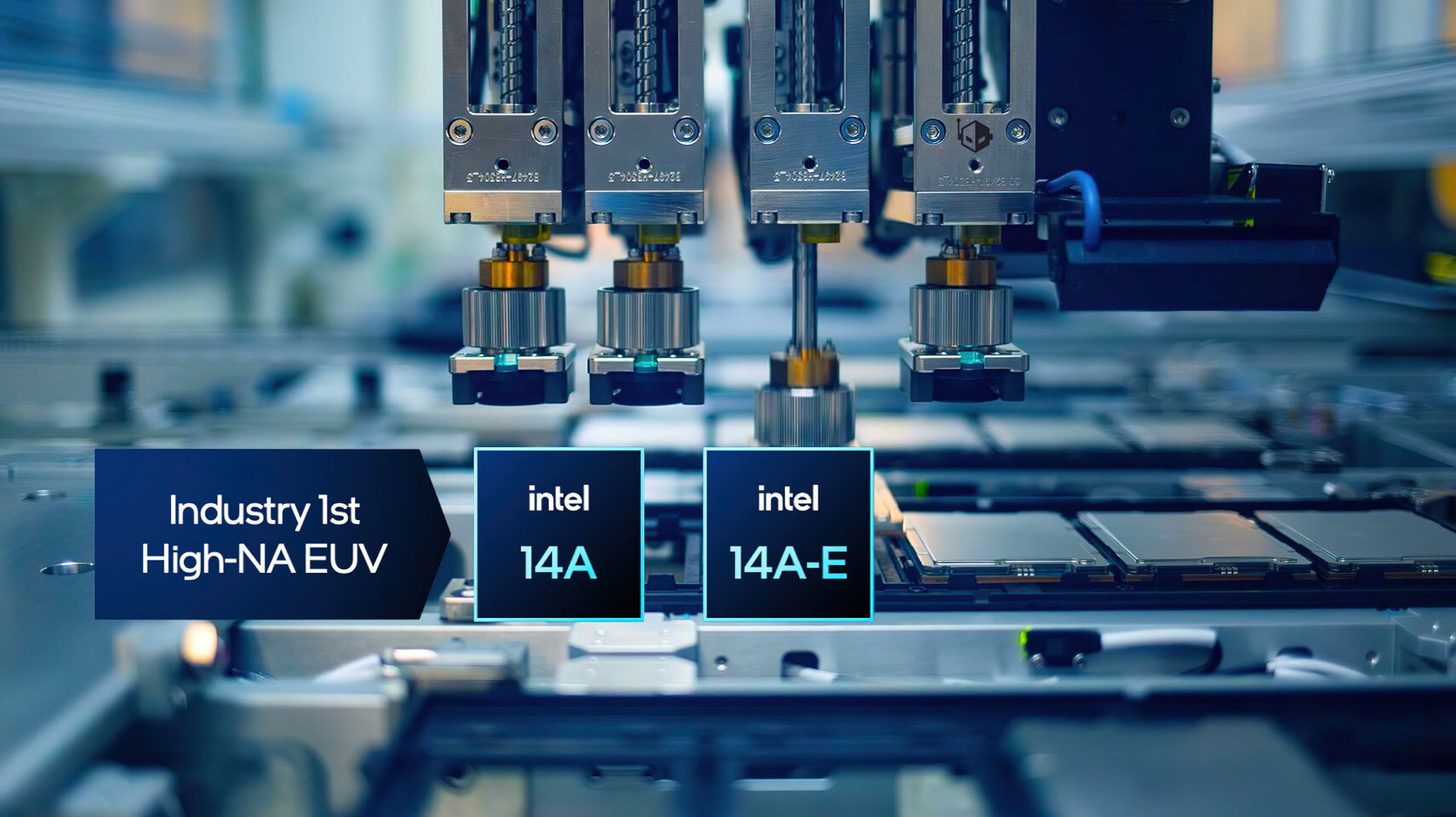
Higher Wafer Costs Driven by High-NA EUV Technology
According to Zinsner, the 14A node will be more expensive than its predecessor, 18A, primarily due to increased wafer costs. While the overall investment required for 14A is not dramatically higher, the adoption of High-NA EUV (Extreme Ultraviolet) lithography tools is a significant factor in the cost increase. Intel is expected to deploy the advanced Twinscan EXE:5200B machine, which carries a price tag of $380 million. This state-of-the-art equipment enables finer patterning and improved chip density, but its high cost means Intel will need to adjust wafer pricing, especially if the 14A node is to attract external foundry customers.
Performance and Efficiency Gains with 14A
Intel projects that the 14A process will deliver substantial efficiency improvements over 18A. The company estimates a 15-20% increase in performance per watt, or a 25-35% reduction in power consumption. These gains are the result of several key process innovations integrated into the 14A node.
One of the major advancements is RibbonFET 2, an update to Intel’s gate-all-around transistor architecture, which enhances current flow and switching speed. Another innovation, PowerDirect, relocates the power delivery network to the backside of the chip, allowing supply rails to feed transistor sources and drains more directly. This change reduces resistance and improves overall power efficiency.
The 14A node also introduces Turbo Cells—taller, high-drive cells embedded within compact standard-cell libraries. Turbo Cells are designed to optimize critical timing paths, enabling higher CPU and GPU frequencies without significant increases in chip area or power consumption.
Advanced Lithography and Future Scalability
While the 18A node relies on more advanced lithography tools to achieve higher resolution and avoid multi-patterning, 14A takes this a step further with the integration of High-NA EUV technology. This approach not only supports greater scaling but also positions Intel to deliver next-generation performance and efficiency for both internal products and potential foundry clients.
As Intel continues to innovate in semiconductor manufacturing, the 14A node represents a significant milestone, combining cutting-edge process technology with a focus on performance, power efficiency, and scalability.