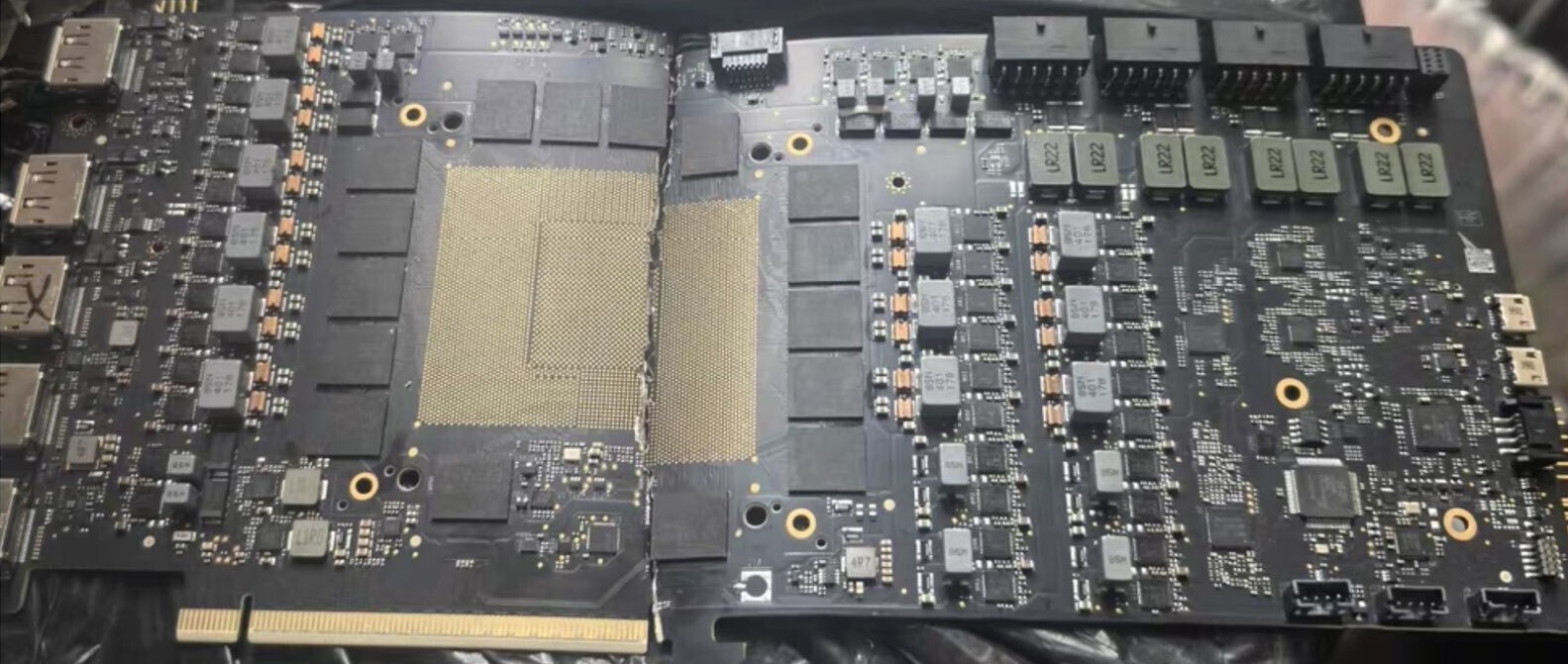
Imagine if the NVIDIA GeForce RTX 5090 GPU had access to not just one, but four 16-pin power connectors. This would result in drawing much less power per connector, reducing the risk of overheating in some cases. The power input to the GB202 could potentially scale up to 2,400 Watts. NVIDIA recently tested this configuration with their leaked engineering sample of the GeForce RTX 5090 GPU. The image below shows a PCB that was damaged during testing.
Around the edges of the card, you can see various features such as USB headers, pin test points, and diagnostic connectors. These are common in development samples but are usually removed from retail models. On the I/O bracket, there are five display outputs, which is more than what is typically found on a gaming card. This indicates that NVIDIA was testing the output strength and signal quality under different loads.
As the back side of the board is not visible, it is uncertain whether the chip belongs to the GeForce RTX 5090 series or the RTX PRO 6000 Blackwell variant. However, it is likely an extremely early sample of the RTX 5090 before mass production commenced.